This article elaborates the whole design process from schematic capture to PCB layout. This also introduces some of the Quadcept features used in each design phase to design your PCB layout with Quadcept.
Overview : PCB Design Process
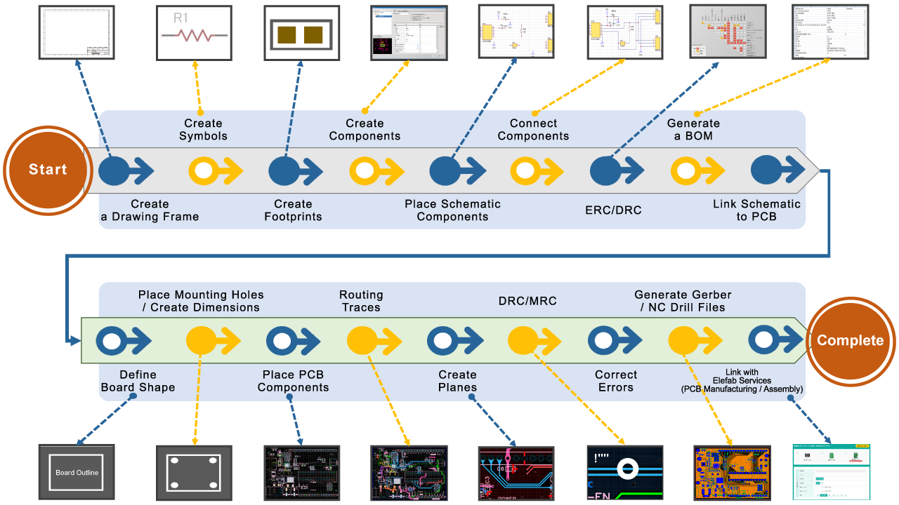
The following image shows the basic PCB layout and design steps.
How to Design a PCB Layout
Creating a Drawing Frame
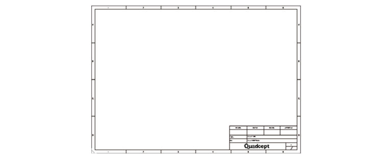
A drawing frame is a schematic template to create a schematic. Quadcept offers various sizes of schematic templates, and you are able to start your design without having to create it from scratch. If you want to unify the format within your team or customize the attributes on it, you can also build a new template through the drawing frame wizard.
Creating a Schematic Symbol
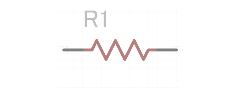
A Quadcept component can be created by linking component models and adding suitable component parameters. To start a schematic design, you first need to create a symbol that represents the component on the schematic sheet.
Creating a PCB Footprint
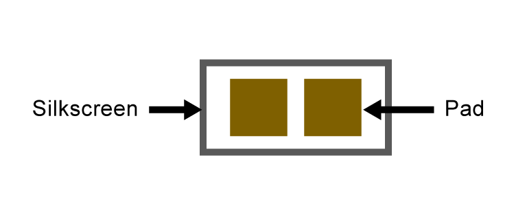
The next step is to create the components to be used in the PCB layout. The component model used for PCB design is called “footprint”. A PCB footprint is created by placing pads providing the connectivity (brown area) and silkscreen used to identify the component shape and position (gray area).
Silkscreen is placed on a silkscreen layer. The line of silkscreen is recommended to be between 0.15 mm and 0.2 mm.
Creating a Component
A Quadcept component is created by linking symbol and footprint models and adding component parameters. Component parameters describe features of electronic parts such as manufacturer name, part number, rated power and operating temperature. For a component name it is recommended to register an official part number such as “MCR03ERPF3001”.
[Sample] Manufacturer Name : ROHM / Part Number : MCR03ERPF3001 / Rated Voltage : 50V
Placing Schematic Components
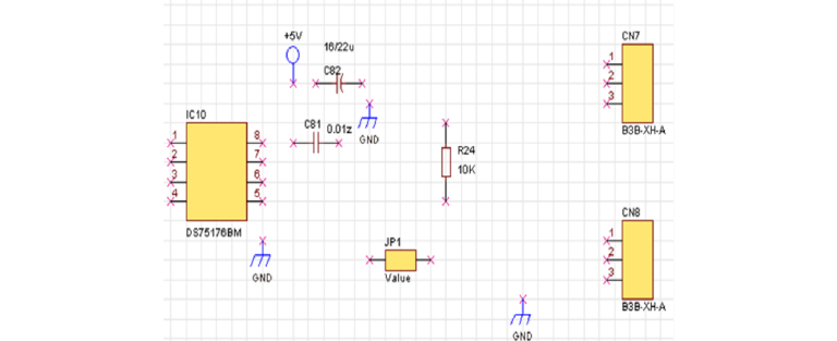
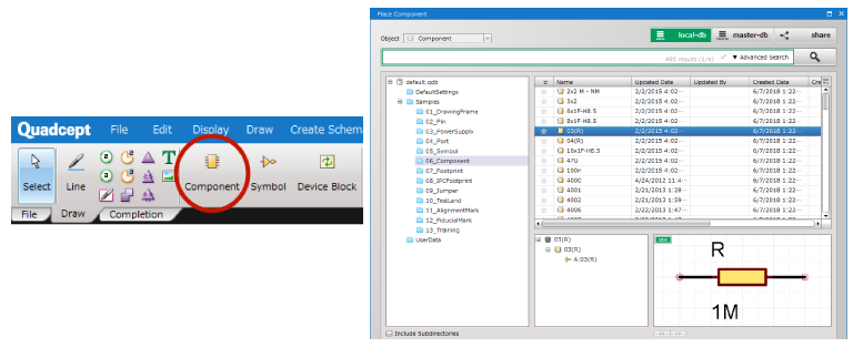
After you have prepared a schematic template and components, the next thing to do is to place schematic components on a schematic sheet. Quadcept supports fuzzy search, and the components you have created can be easily found by the keywords such as a part number and an attribute. After you have found your required component, you can enter placement mode for the component by a double-click. Making a click on the design sheet will allow you to place the component.
Wiring
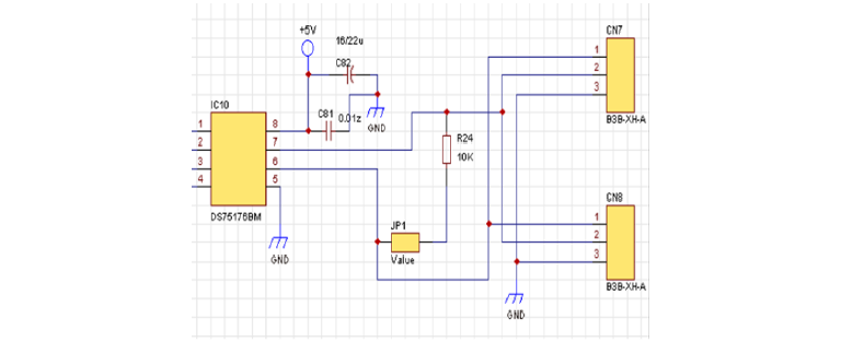
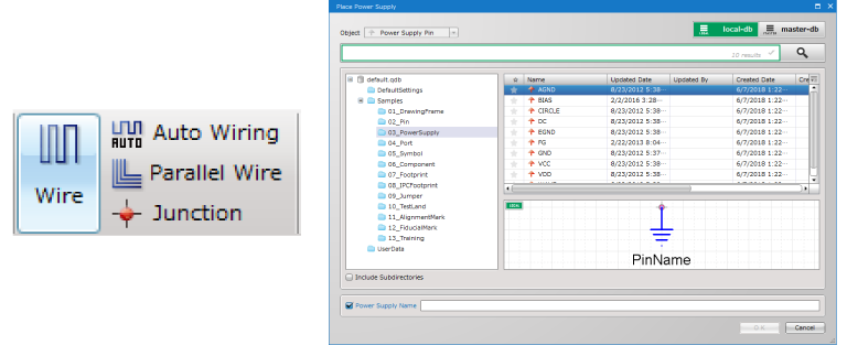
Now you are ready to connect the components. A wire is used to create electrical connectivity between components on a schematic. Selecting the Wire icon in the Draw tab of the ribbon menu and clicking on a pin point of a component will start a wire. You can anchor a vertex point by making a click while placing it. Clicking on the destination pin point will complete placement of the wire, and the components will be electrically connected.
If you want to place a power / GND symbol while placing a wire, you can do it through the Add Power/GND command. Right-clicking to select the command and double-clicking your required model from the 03_PowerSupply folder in the Place Power Supply dialog will allow you to place that symbol.
In Quadcept, there are some more useful features that help wire placement such as “Auto Wiring” and “Parallel Wire”. For details see the online manual.
Verifying Your Schematic Design with ERC/DRC
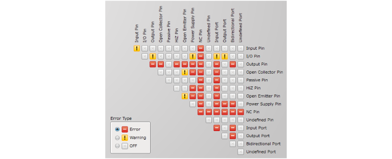
After you have finished designing your schematic, you may want to run the ERC / DRC for verification. ERC, short for Electrical Rule Checking, is used to check for violations concerning the connections between the components on the schematic sheet.
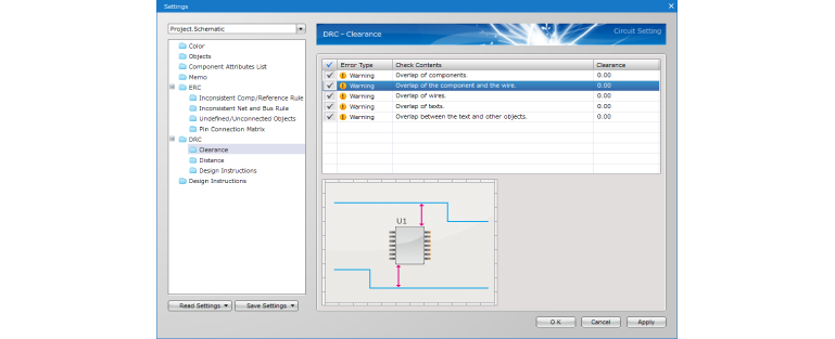
DRC, short for Design Rule Checking, is used to check for violations concerning the schematic layout. The ERC / DRC is run by selecting [ERC/DRC] >> [Run ERC/DRC] in the Completion tab of the ribbon menu. For each setting relating to the ERC / DRC you can access it by selecting [ERC/DRC] >> [ERC/DRC Settings] in the same tab.
Generating a BOM File
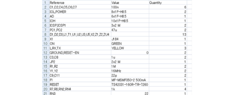
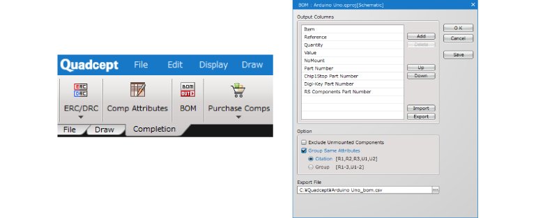
The final step for schematic capture is to generate a BOM file for part procurement. The items exportable for a BOM file can be specified from the component attributes added when the components are created. To make it easy to set up the export columns and avoid any mistakes it is recommended to use the same attributes when creating components.
- Select the [BOM] command in the Completion tab of the ribbon menu.
- In the BOM dialog, you can edit component attributes to be exported.
- Clicking on the [OK] button will export a BOM file in CSV format.
The menus [Comp Attributes] and [Purchase Comps] located at both sides of the BOM command are useful for part procurement. These commands enable you to link your design components to real-world parts provided by Digi-Key, Mouser Electronics, Chip1Stop, RS Components and CoreStaff, and access those suppliers’ live component data such as pricing and stock information in real time during design.
Linking the Schematic to the PCB
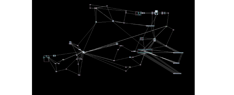
After your schematic design is completed, it’s time to start the PCB design. Quadcept is an integrated design environment, where the schematic and PCB are interlinked and can be accessed concurrently.
To transfer your schematic information to the PCB design document select the Transfer to PCB command in the Completion tab of the ribbon menu. Note that this command cannot be run if no footprint models are linked to the schematic components.
- Make sure that footprint models are linked to schematic components.
- Select the Transfer to PCB command in the Completion tab of the ribbon menu.
- Linked footprint models will be automatically placed on a PCB design document according to the layout of the schematic.
- Connection information is called “net”, and it will be indicated by a white line.

Defining the Board Size

After you transfer your schematic information to the PCB design sheet, the next thing to do is to define the board size. When you specify the board outline, it is recommended that the bottom left corner of the board be at the origin point (X:0, Y:0).
- Set the line width to 0.1 ~ 0.2 mm (recommended).
- Specify “Other” as “Current Layer”.
- Specify “Board” as “Layer Type”.
- When drawing a board outline, it is recommended that the bottom left corner of the board be put at the origin point (X:0, Y:0). The origin point can also be moved after the board outline is defined.
- Draw the board outline with drawing tools such as [Line], [Rectangle] and [2 Point Circle] in the Draw tab of the ribbon menu.
- The board size can be specified in the Property window located at the left side of the screen after the board outline is drawn. The following image shows the board outline created at a size of 57 x 57 mm.

Placing Mounting Holes

After you define the board size, place mounting holes as needed. They are placed by using pads.
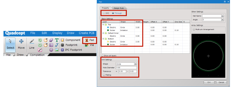
- Select the Pad command in the Draw tab of the ribbon menu.
- The Pad dialog will appear. Choose [Through] as its pad type at the top of the dialog.
- Choose [Circle] in the Shape fields and specify a diameter in the Width fields for Top / Bottom / Default Inner. The sample below shows a mounting hole of 3 mm.
- The drill settings located below are important. Choose [Circle] in the Shape field, and specify a hole diameter in the Hole Diameter field (3 mm in the following image). Remove the check for the Plating option.
Placing Dimensions
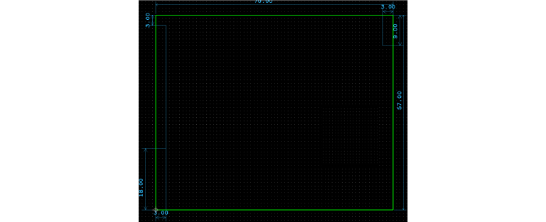
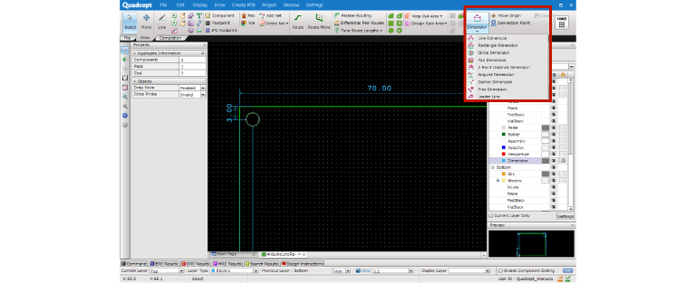
The next step is to place dimensions for the board outline. Quadcept supports 9 types of dimensions which help you create dimensions easily and smoothly. Each dimension menu can be accessed from the Draw tab of the ribbon menu.
Placing Components
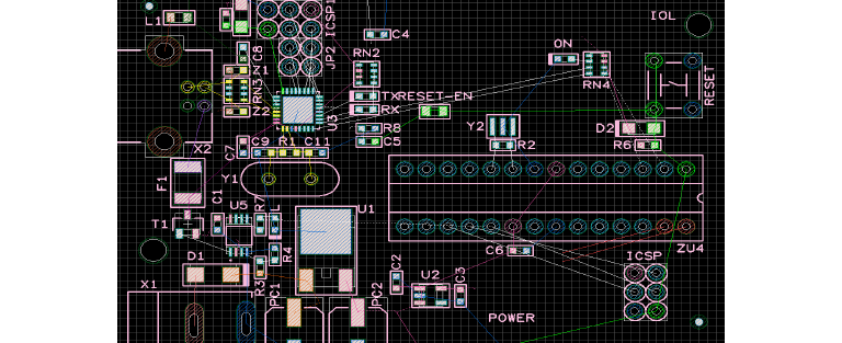
Now, you are ready to place components.
Basic Actions
After selecting the Select command in the Draw tab of the ribbon menu and dragging a component placed on a PCB sheet, that component will be attached to the cursor and you will enter component placement mode. You can also enter that mode by pressing the Enter key on the keyboard after selecting the component. Move the cursor to your desired position and click to place it.
Move Mode
The Move command can be accessed from the Draw tab of the ribbon menu. With this command you can enter component placement mode just by clicking on a component. This also allows you to hold the origin point of the component as a reference point for moving.
Rotating / Mirroring
Each component can be rotated or flipped from the Move/Rotate/Mirror command in the right-click menu while moving components. The Rotate and Mirror commands can also be performed by pressing the R and M keys on the keyboard respectively.
Routing Traces
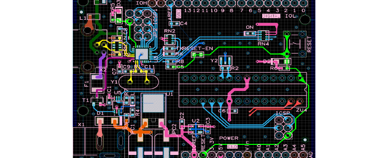
When you are done placing components, now it is time to route your traces. The following menus are used to perform this step. To route a signal select the Route command and then click on a component pad or connection line (rats nest) on a PCB sheet.
You can see available features in the context menu shown by right-clicking while routing. Through that menu, you are able to perform various actions such as changing line width and placing jumper components.

During routing, you can switch layers with the Change Layer command in the right-click menu or the Tab key on the keyboard. The current layer and grid can be checked and changed in the Status Bar located at the bottom of the screen.

Creating Planes
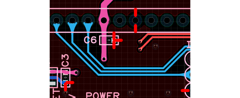
Planes are created to implement large copper areas for power and ground nets.
Net information is necessary for planes.Planes are frequently created on the Top / Bottom layer. In the case of multi-layer PCBs, they are also placed in the inner layers. Create them according to your design.
Plane Type
| Dynamic Plane | Automatically connects to objects with the same net name according to the design rules you define, and creates clearance from objects with different net names to prevent short circuits. |
| Static Plane | It fills the area you draw. It is suitable for reinforcing the route. |
Each plane drawing menu can be accessed in the Draw tab of the ribbon menu.
Each plane drawing menu can be accessed in the Draw tab of the ribbon menu.
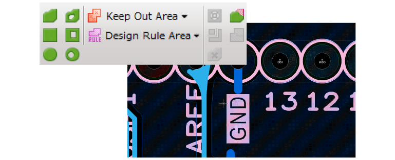
Select one of the menus according to your required shape, and click on a net object such as pad or route, which has the net you want to assign to the plane. After specifying the net draw the plane onto the area you want to apply the copper to.
Verifying Your PCB Design with DRC/MRC
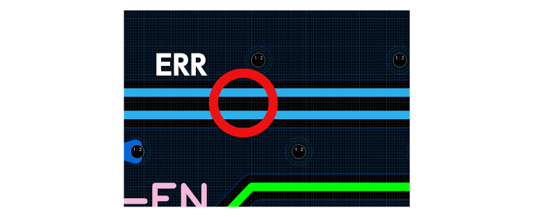
When you are done routing your traces, verify your circuit board layout by running a DRC / MRC. DRC, short for Design Rule Checking, is used to check for violations such as a short circuit between traces based on design rules you define. MRC, short for Manufacturing Rule Checking, is used to check for violations such as mismatched text angles from the perspective of manufacturing.
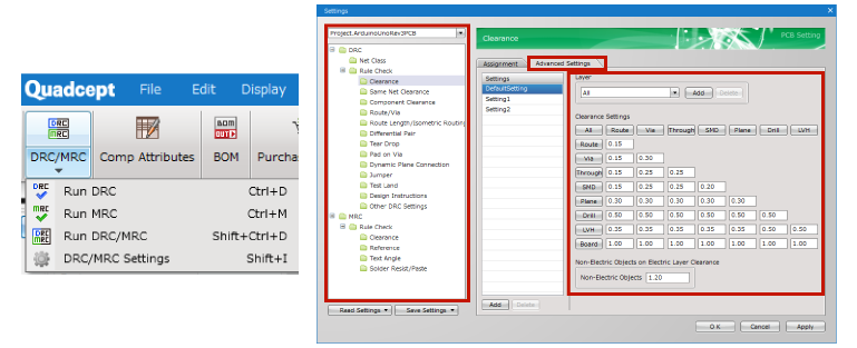
- Select [DRC/MRC] >> [DRC/MRC Settings] >> [Clearance] from the Completion tab of the ribbon menu to open the Clearance settings, and define the clearance between each object there.
- Clearance is a distance between any two objects on a copper layer. For this setting define the minimum clearance allowed between them.
- Once you have completed the settings, click on the Run DRC/MRC commands and verify the whole design. A DRC and MRC can also be run separately.
Correcting Errors
If any errors are found through a DRC / MRC, you will need to correct them to complete your design.
When it is hard to modify your design due to the existence of planes, pressing the [K] key on the keyboard will display only the outline and make it easier to work on the errors.
Even when you have placed any objects within the areas of a dynamic plane, you can rebuild it to avoid short circuits by running the Rebuild Plane command.
Generating Gerber / NC Drill Files
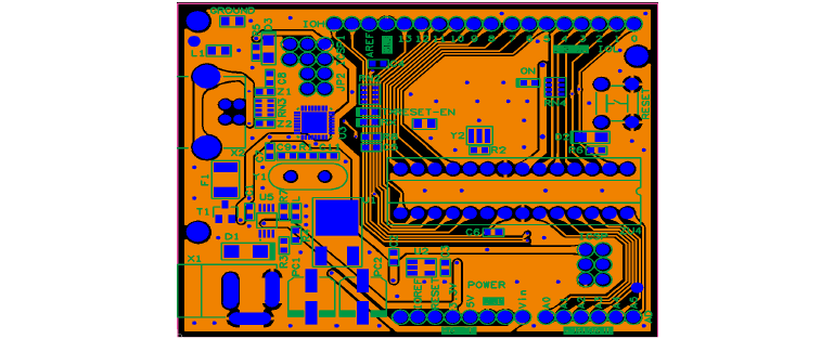
Gerber is the most widely used file format for PCB manufacturing. It contains all of the details on your individual layers. The NC drill file conveys drilling information. It is used to specify the location and size of each of your drill holes.
Those files are necessary for PCB manufacturing. Pay attention to the tiniest details when you export them, as any mistakes in this phase may lead to costly repercussions in manufacturing.
Settings
Export
Linking with Elefab™️ Services
Elefab™️ is a one-stop service for PCB design, fabrication and assembly Quadcept provides on cloud.
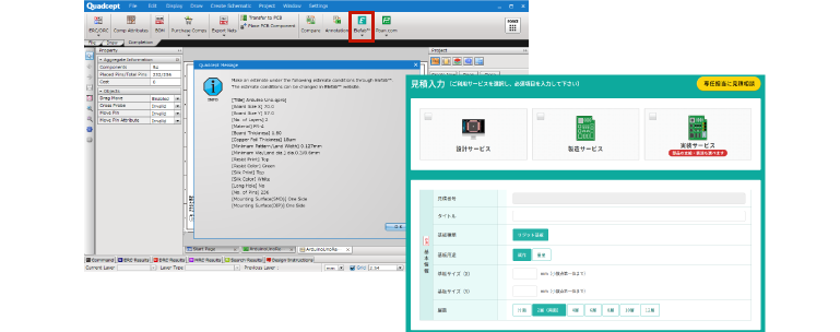
Quadcept and each Elefab™ service are interlinked, and you can get an instant PCB quote during or after design just by clicking on the Elefab™ button in the Completion tab of the ribbon menu.
Your created quote can also be saved in the system, and you can instantly place an order when you need.
